
Sending PCB designs off to China? Old news! Etching copper clad boards at home with some nasty chemical? Who’s got time for that?! The latest and greatest way to prototype circuit boards is with the Voltera V-One PCB Printer. Although it's not the cheapest machine, it's the perfect tool for my electrohaptic feedback project. I'm specifically using it for the electrode array that attaches to your fingertip, where I'm looking to create a flexible substrate for maximum comfort and effectiveness.
The Voltera V-One is a 3D printer which uses conductive inks to print conductive ink. It can be used to quickly prototype simple designs and means that to get a purpose built board which doesn't use stipboard or veroboard can be done quickly and relatively easily. Traditionally, it is used to print single layer, or sometimes dual layer PCBs onto either a rigid substrate, like FR4, or onto a flexible substrate, like Kapton film. To make the dual layer boards, the V-One uses drilled holes and rivets and so it is only possible to create dual layer rigid boards leaving flexible boards on just a single side.
For simple designs these limitations are fine and are simple enough to work around a lot of the time. If you are prototyping simple boards, its a powerful tool for teaching both circuit design and additive manufacturing in the same machine however, once you need a second layer (or more) the process becomes much more difficult and even more limitations are introduced. After using this machine for a few months, I've learnt its quirks but also the secret power it holds once you remember what this machine essentially is, a 3D printer!
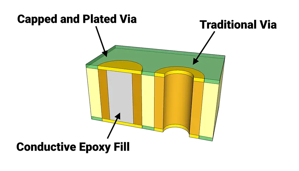
The Voltera V-One boasts some pretty impressive specs stating that it can print down to trace widths of 0.2mm (8mil) and can do pin-to-pin pitches of 0.65mm (26mil). It can print on rigid boards or flexible substrates too - exactly what I need. Another feature of the V-One that isn’t explicitly stated is the ability to use other liquids like, for example, a material that would allow vertical stacking of layers such as resin. Now, the utility of this isn’t immediately obvious; why wouldn’t you just use vias to go from one side of a board to the other? In the case of flexible substrates, this option can include using rigid rivets which would decrease the flexibility of a small board. Another issue is when you want as much surface area in a small space as possible, as is the case with the electrode array I’m designing, because in the middle of a conventional via is a airgap. There is a process called "via-in-pad" that can be used to overcome issues like using vias in tight spaces and the airgap in the centre. The process for creating this feature is more complex than a regular via as there are extra steps involved in the fabrication process.
Using the V-One, I can print the traces and pads on just a single side of rigid or flexible material, then print a layer of resin to act as an insulator, then finally print the top layer of electrode pads that would be in contact with the finger. To connect the layers, I can utilise a similar process to the via-in-pad, but with a much lower cost and complexity as I'm simply using the V-One as its predecesors intended, as a 3D printer. Using this method also allows me to create blind and burried vias, another feature that is usually reserved for only high end PCB fabrication processes.
The process was something that I had to tune so that I didn't break too many of the fragile nozzles that are used on the V-One. For the conductive inks, I continued to use the high precision machined nozzles but for the resin, I used a similar sized needle with the end cut down to fit properly onto a cartridge.


After developing my method, I was left with something that goes like this:
The first conductive ink layer is printed onto the substrate like normal. For a 2 layer design, this would be the bottom layer which has additional reference points so that additional layers can be aligned properly.
Bake the board to the settings of the conductive ink.
The next layer is the vias which should be loaded up and aligned to the pads below. This layer is then printed at roughly a 0.15mm layer height so that it can be safely printed on top of the rough surface of cured ink.
Bake (another 45 minutes of waiting)
Now the resin layer will be printed by aligning the layer with the reference points and printing at the same height as before, roughly 0.15mm.
The layer is closely inspected to make sure that there is no runover of the resin to the vias but that the resin is completely covering lower layers.
Blast the UV curable resin with some UV rays (courtesy of a high power UV torch, the sun also works).
The final layer can be printed. In my design, this is the top layer that has the pads which will be in contact with the fingertip. Align with the reference points and print at roughly 0.15mm.
Bake!
Test all the points for continuity and hope that your hard work has paid off!
After these steps, you should be left with something that resembles the design you were expecting. To make sure that all the layers were doing their jobs, I sacrificed one of my first test boards to get a cross-section.


Now, it wasn't all smooth sailing and there were/are definitely some issues with the whole process. The main problems are down to the V-One being a relatively unsofisticated piece of equipment. By that I mean that it lacks some features that would make using the machine much easier and projects like mine more abundant. In terms of hardware, some kind of camera system would be incredibly helpful as aligning the layers (on points that are just 1mm^2) is difficult to say the least and caused shorts on at least one of my test boards because of poor alignment.
I guess you could say that alignment is human error, but when it comes to the software there are 'features' that just don't work so well in practise. My two main complaints here are the calibration sequence that forces you to print over the top of your work piece and the seemingly completely random Z probing. I understand that the calibration sequence was not built for my purposes but I would appreceiate the ability to move it to another area of the board. As for the Z probing, I have no solution other than to request that the probing should be the same between probings of the same design.

As an experiment, I also played around with some black UV-curable resin and found that it could be used to create text. With the limited time I spent tinkering with the Z-height and flow settings, I was able to get text that I would say is legible at 100mil height but I think this could be improved by using a smaller nozzle, slower speeds and a lower layer height.
Unfortunately for these tests, it looks like a lower layer height is a requirement as even after curing with a 10W UV torch for twice as long as usual, only the outer layer of the text was cured leaving uncured resin shielded inside.
Overall, the Voltera V-One proved to be a useful tool in creating the custom boards I hope it could make. While there were some challenges with the machine's lack of advanced features, such as a camera system, the process was simple and repeatable. By sacrificing one test board to get a cross-section, I confirmed that all layers are properly aligned and that the interlayer connection looks almost seamless. With some improvements to the machine's calibration and probing sequences, the V-One could become even more user-friendly and capable of producing more complex designs. Despite its limitations, the V-One has proven itself to be worth more than it's often given credit for. As the NOVA, the bigger brother to the V-One, is now available, I hope that it can cover all the short comings and that more people can develop this process in the future.
Comentarios